Basic Troubleshooting - Reading Schematics
When we first look at the printed circuit board (PCB) of an Atari ST or similar retro computer, it can be quite daunting. All those chips, connected god knows how, what am I to do!!
Well all is not lost, because many older machines, the ST range included, have original schematics available in PDF form, many of which are available right here on exxos forum: Useful schematics
Unlike datasheets, schematics show more than just one component, they show all components within a machine and how they are logically connected together. Armed with both the datasheets and schematic, we are in a very strong position to understand how each device is connected. Also of importance, the name of the component is indicated, such as U39 or R59, which can matched with the silk screen guide printed onto the PCB itself.
There are some considerations to make when looking at schematic diagrams though.
The first is that it is a logical diagram, and not one of physical connections. This is important to understand, because whilst a datasheet will show actual physical connections to a chip, a schematic will show those connections in the way they are logically connected. This picture is an example of this:
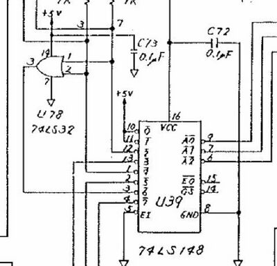
What we can see here is a chip labelled U39 and labelled as a 74LS148, however if we compared it to the datasheet view:
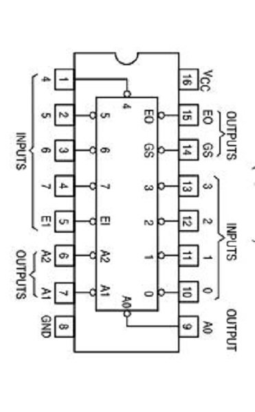
We can see that the simple arrangement of pins on the datasheet does not match the schematic. Why is this?
The reason is that in order to show all the connections for each chip, it is easier to draw them in a logical manner that shows the connections and pin numbers as a representation of a chip, rather than try and connect all the pins as it would be physically connected.
Why do this? What is important is to see what is connected to where, rather than how things are physically connected. By doing this we can easily trace on the real PCB because we know that on chip A, pin 5 connects to pin 16 on chip C.
Another important point from this image is that U39 and U78 are illustrated differently. U39 is a logical representation, whereas U78 is simply represented by a logic gate, though importantly, the physical pin numbers are still present.
This is an example showing some connections from the 68000 on the left, to the GLUE on the right:
This in no way represents the physical connections, because the pins are just not laid out like that, but we can say for sure that pin 10 on the 68000 connects to pin 31 on the GLUE. Because we also have the data sheets we can now relate the physical pins to their real life connections. If we suspected a problem here, we could use a continuity test to confirm that the connection between those pins was good.
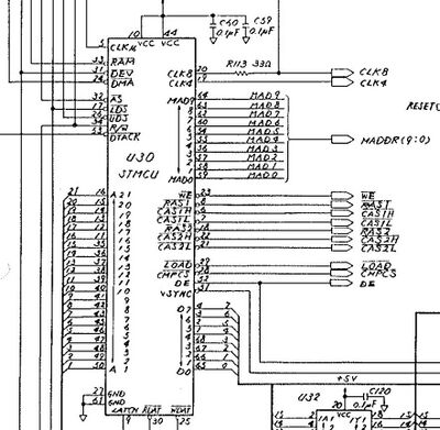
Another consideration when looking at schematics is how things like address and data lines are handled. Here we see one of the STs many chips with both address and databus connections:
Once again, the pin numbers are numbered as per the datasheet, but in the schematic, not where you'd find them on the actual chip. What is key here is that to draw ALL of the address and data lines would take up a mass of space and make the schematic huge. So what is done is that initially at the chips,they all pop out (A1-A21 and D0-D7), but as soon as possible they merge into a single line representation of the address and data bus. This saves time and space and is a technique that helps simplify the schematic.
The important takeaway is that at each chip these buses are shown and this again allows us to easily understand where connections are being made chip to chip. This type of representation for multiple bus connections is standard on most schematics.
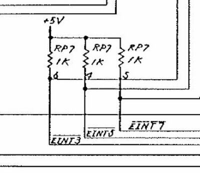
Finally, it should also be noted that when it comes to standard components like resistors and capacitors (And anything else too), these are represented in schematics as standard electronic symbols.
Here we can see three 1K resistors that form part of the resistor pack RP7, all identified using the standard symbol for a resistor:
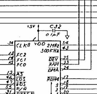
And here we see capacitor C32, again represented as a standard electronic symbol:
Note that C32 is a good example of how sometimes scanned schematics can lose information. Is it 1uF or 0.1uF? Bear these foibles in mind when navigating your schematics.
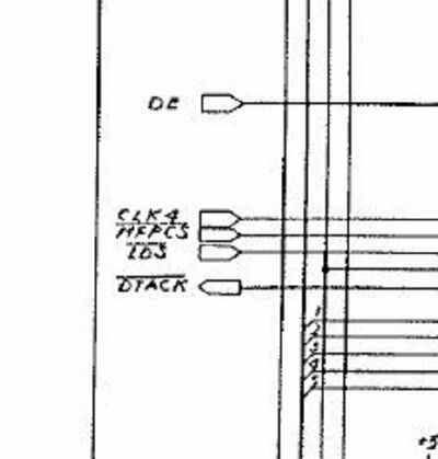
You will also see that many are multi-page documents, so it's important to view in the correct page order and understand that connections between each page are shown on page edges like this:
On the whole you will find that they represent a great roadmap and will show you how everything is supposed to be connected, which component is which, and in the case of discrete components, what values to expect.

